CNG solves one of the biggest challenges with graphene-based nanoelectronics
Researchers from the DNRF’s Center for Nanostructured Graphene (CNG), together with researchers from Japan, have, for the first time, solved one of the biggest challenges with the construction of nanoelectronics based on the “miracle material” graphene. The results were recently published in the renowned scientific journal Nature Nanotechnology.
In a new study published in the scientific journal Nature Nanotechnology, a research team from the Center of Excellence CNG, DTU, and Aalborg University in collaboration with researchers from the National Institute for Materials Science, in Japan, is the first to solve one of the biggest challenges with the construction of efficient nanoelectronics based on the “miracle material” graphene. The problem is that the material’s properties are vulnerable and easily affected by irregularities that occur when working with the development of graphene. But now, two post-docs from CNG have found a way to avoid the problem.
Even miracle materials have a downside
Graphene is the thinnest known material, consisting of one layer of carbon atoms arranged in a hexagonal lattice. The material is popularly considered a “miracle material” because it is transparent, 200 times stronger than steel in relation to its thickness, and an excellent conductor of both heat and electricity. The properties of this ultra-thin, two-dimensional material mean that graphene, in theory, is ideal for creating new forms of electronics, which are both faster and more energy-efficient than the electronics we have today. For this reason, researchers for the past 15 years have tried to use this wonder material for the manufacturing of electronics at nanoscale. But even miracle materials have a downside.
“Graphene is a fantastic material, which I think will play a crucial role in making new nanoscale electronics. The problem is that it is extremely difficult to engineer the electrical properties,” said Peter Bøggild, professor at CNG and one of the article’s authors.
By patterning graphene at nanoscale, researchers are able to tailor the properties of the material, which is crucial for making transistors and sensors. At the same time, nanolithography – fabricating nanoscale structures and materials – has proven to be one of the most powerful methods behind electronics that makes today’s computers and communication technology work. But graphene is so thin that all of its atoms are very important for the material, which means that even the smallest irregularities can destroy its properties.
“When you make patterns in a material like graphene, you do so in order to change its properties in a controlled way – to match your design. However, what we have seen throughout the years is that we can make the holes, but not without introducing so much disorder and contamination that it no longer behaves like graphene. It is a bit similar to making a water pipe that is partly blocked because of poor manufacturing. On the outside, it might look fine, but water cannot flow freely. For electronics, that is obviously disastrous,” said Professor Bøggild.
Post-docs break nanoelectronic curse
But now the problem seems to be resolved. Thanks to a method developed by two post-docs from CNG, Bjarke Jessen and Lene Gammelgaard, the researchers can encapsulate graphene inside another two-dimensional material – hexagonal boron nitride, a non-conductive material often used to protect graphene’s properties.
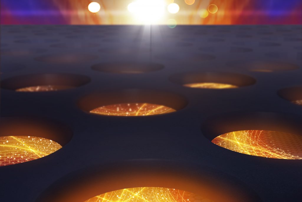
After the protecting the graphene with hexagonal boron nitride, the two post-docs and the rest of the research team used a technique called electron beam lithography to carefully pattern the protective layer of boron nitride and graphene below with a dense array of small holes. The holes have a diameter of approx. 20 nanometers, with just 12 nanometers between them; however, the roughness at the edge of the holes is less than 1 nanometer. This allows 100-1000 times more electrical current to flow than had been reported in such small graphene structures.
“We have shown that we can control graphene’s band structure and design how it should behave. When we control the band structure, we have access to all of graphene’s properties, and we found to our surprise that some of the most subtle quantum electronic effects survive the dense patterning; that is extremely encouraging. Our work suggests that we can sit in front of the computer and design components and devices – or dream up something entirely new – and then go to the laboratory and realize them in practice,” said Bøggild. He continued:
“Many scientists had long since abandoned attempting nanolithography in graphene on this scale, and it is quite a pity, since nano structuring is a crucial tool for exploiting the most exciting features of graphene electronics and photonics. Now we have figured out how it can be done; one could say that the curse is lifted. There are other challenges, but the fact that we can tailor electronic properties of graphene is a big step towards creating new electronics with extremely small dimensions.”
More information can be found at the website of Technical University of Denmark here.